TSMC’s Unorthodox Optical Leap – IEEE Spectrum
In the race to an all-optical AI data center, a major player has now placed a bet on a different horse. Semiconductor manufacturing giant TSMC announced that it will work with Sunnyvale startup Avicena to produce microLED-based interconnects. The technology is a pragmatic twist on replacing electrical connections with optical ones to meet the high needs of communication among an increasing number of GPUs in a low cost, energy efficient way.
Thanks to the computational demands of large language models and their cousins, AI clusters are facing unprecedented requirements regarding amounts of data, bandwidth, latency, and speed. Sooner or later, the copper wires that connect processors and memory within a single AI data center rack will have to be replaced with optics. “There’s a huge push to get optical connections as close to the board as possible,” says Lucas Tsai, a vice president at TSMC.
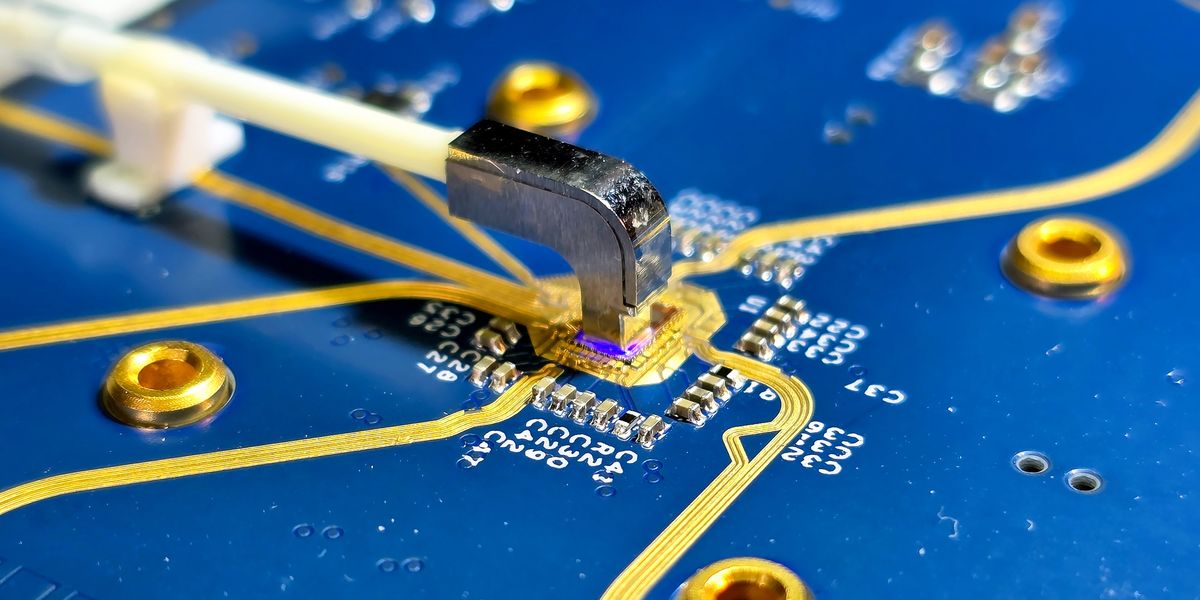
Avicena offers a unique approach, using hundreds of blue microLEDs connected through imaging-type fibers to move data. The company’s modular LightBundle platform avoids problems with lasers and their associated complexity that threaten the reliability, cost, and power consumption of other optical chiplets. Tsai says “it’s very unorthodox!” But it is ideal for these short distance applications, and that’s precisely what makes it interesting.
Laser-free
Optical connections today carry vast amounts of data tens to hundreds of meters across data centers at very high data rates. Traditionally, a pluggable module connects the optical fiber to the rack, where it converts between electrical and optical signals. Companies are making strides toward getting rid of these energy inefficient pluggable transceivers using co-packaged optics (CPO), which instead perform electrical-optical transformations adjacent to the silicon chip itself. Commercial versions exist for the network switch, and prototypes are making strides toward the GPU. The most prominent optical chiplet designs encode electronic bits onto multiple wavelengths of light using lasers and modulators.
However, the main challenge for laser-based optical interconnects is the laser itself. The laser and fiber attachments have caused the biggest problems in terms of reliability, manufacturing, and cost. Moreover, a single optical fiber that hosts dozens of GPU-to-switch links in the form of multiple wavelengths suffers from computational overhead: it’s far simpler to pipe each data lane down a separate physical channel than to electronically parse one big channel later on.
That’s where Avicena comes in. Instead of sending a multi-wavelength laser down an optical fiber and then parsing it into individual channels, the LightBundle interconnect links hundreds of blue microLEDs to a photodetector array via multi-core imaging fibers—one for each 10 GB/s data lane. The transmitter acts like a miniature display screen and the detector like a camera. “We’re doing optical interconnects without the complexity of lasers,” says Avicena CEO Bardia Pezeshki.
A simple optical link with just 300 pixels at 10Gb/s per lane can extend over a 10m distance, carrying a net total of 3 Tb/s. Since displays and cameras can scale to millions of pixels, the technology can scale to much higher data rates at much lower energy and much higher density than copper wiring.
Mature industry
One major advantage touted by Avicena is that their technology harnesses LEDs, cameras, and displays: all mature industries. “We can scale our approach to the volumes and costs required much more rapidly than if we were developing new building blocks,” says Pezeshki. Even though silicon photonics has a thirty-year head start on optical interconnects, they have to develop new components like ring resonators and comb lasers. “It takes a lot of time for these things to mature,” he says. In contrast, the LightBundle interconnects design requires only minor modifications to existing camera and display technologies.
That’s one main reason that TSMC signed up to produce the photodetector arrays for Avicena’s optical chiplets. “LEDs is a mature industry already, there are a lot of consumer products,” Tsai says. LEDs are of course lower power than lasers—but for, say, 10-meter distances within and across a rack, that’s enough. “There’s a potential that it will be a lot cheaper, and by nature you have a lot of redundancy,” says Tsai.
Avicena’s results are already “blowing away” what silicon photonics can do, according to Pezeshki. The LightBundle prototype has already demonstrated sub-pJ/bit energy use for the whole link, where other optical approaches “are struggling to show” 5 pJ/bit energy consumption.
Pezeshki acknowledges that Avicena has a ways to go to build and scale the product. But “the combination of showing great results together with using mature building blocks is winning over converts,” he says.
From Your Site Articles
Related Articles Around the Web